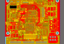
Introduction to FPGA: Architecture, Verilog, and VHDL Basics
Abstract: Field Programmable Gate Arrays (FPGAs) are an essential component of modern electronic systems. This article will provide a comprehensive introduction to the structure of FPGAs, along with basic examples in Verilog and VHDL for beginners.
Introduction: Field Programmable Gate Arrays (FPGAs) have revolutionized electronics by providing a flexible and configurable hardware platform. An FPGA is essentially an integrated circuit that can be programmed to perform a specific function after manufacturing, making it highly versatile and adaptable for various applications. This article will provide an overview of the architecture of FPGAs, along with basic examples in Verilog and VHDL to help beginners understand how these programming languages are used with FPGAs.
FPGA Architecture: At its core, an FPGA is composed of an array of logic blocks, input/output (IO) pins, and interconnect resources such as routing channels or switches. These logic blocks can be configured to perform specific functions, and the interconnect resources allow signals to flow between these blocks. The IO pins connect the FPGA to external devices, allowing data to be transferred in and out of the device.
Verilog for Beginners: Verilog is one of the most popular programming languages used with FPGAs. It is a hardware description language (HDL) that allows designers to describe their designs at a high level of abstraction, making it easier to design complex systems. Here's a simple example of Verilog code:
module led_blink(output LED);
    input clk;

    always @ (posedge clk) begin
        LED <- ~LED;
    end
endmodule
In this example, we create a module called "led_blink" that takes an input clock signal (clk) and outputs a signal named LED. The "always" block is triggered by the positive edge of the clock signal, which toggles the value of the LED signal every clock cycle. This simple code can be synthesized to an FPGA to create an LED blink circuit.
VHDL for Beginners: Another popular HDL used with FPGAs is VHDL (VHSIC Hardware Description Language). Similar to Verilog, VHDL provides a high-level way of describing hardware designs. Here's a simple example of VHDL code:
library ieee;
use ieee.std_logic_1164.all;

entity led_blink is
    Port (clk : in  STD_LOGIC;
          LED   : out  STD_LOGIC);
end entity led_blink;

architecture Behavioral of led_blink is
begin
    process(clk)
        variable LED_var: STD_LOGIC := '0';
    begin
        if rising_edge(clk) then
            LED <= not LED_var;
        end if;
    end process;
end architecture Behavioral;
This VHDL code does the same thing as the Verilog example, creating a module called "led_blink" with an input clock signal (clk) and an output LED signal. The process block is triggered by the rising edge of the clock signal, which toggles the value of the LED variable every clock cycle.
Conclusion: Understanding FPGAs, Verilog, and VHDL is essential for anyone interested in electronics design or embedded systems development. The examples provided above demonstrate how simple circuits can be described using these languages, making it easier to understand the underlying concepts involved in designing with FPGAs. As you continue learning and experimenting with these tools, you will find that they open up a world of possibilities for creating complex and highly optimized electronic systems.


